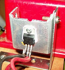
The LM317 is an adjustable positive linear voltage regulator. It was designed by Bob Dobkin in 1976 while he worked at National Semiconductor.
The LM337 is the negative complement to the LM317, which regulates voltages below a reference. It was designed by Bob Pease, who also worked for National Semiconductor.
Specifications

| Symbol | Parameter | Value | Unit |
|---|---|---|---|
| Vout | Output voltage range | 1.25 – 37 | V |
| Vin – Vout | Voltage differential | 3 – 40 | V |
| TJ | Operating junction temperature range | 0 – 125 | °C |
| IO(MAX) | Maximum output current | 1.5 | A |
| IL(MIN) | Minimum load current | 3.5 mA typical, 12 mA maximum | |
| PD | Power dissipation | Internally Limited | W |
| RθJA | Thermal resistance, Junction to ambient | 80 | °C/W |
| RθJC | Thermal resistance, Junction to case | 5 | °C/W |
Without a heat sink at an ambient temperature at 50 °C, a maximum power dissipation of (TJ-TA)/RθJA = ((125-50)/80) = 0.98 W can be permitted.
In a constant voltage mode with an input voltage source at VIN at 34 V and a desired output voltage of 5 V, the maximum output current will be PMAX / (VIN-VO) = 0.98 / (34-5) = 32 mA.
For a constant current mode with an input voltage source at VIN at 12 V and a forward voltage drop of VF=3.6 V, the maximum output current will be PMAX / (VIN - VF) = 0.98 / (12-3.6) = 117 mA.
Operation
Main article: Linear regulatorAs linear regulators, the LM317 and LM337 are used in DC to DC converter applications.
Linear regulators inherently waste power; the power dissipated is the current passed multiplied by the voltage difference between input and output. A LM317 commonly requires a heat sink to prevent the operating temperature from rising too high. For large voltage differences, the power lost as heat can ultimately be greater than that provided to the circuit. This is the tradeoff for using linear regulators, which are a simple way to provide a stable voltage with few additional components. The alternative is to use a switching voltage regulator, which is usually more efficient, but has a larger footprint and requires a larger number of associated components.
In packages with a heat-dissipating mounting tab, such as TO-220, the tab is connected internally to the output pin which may make it necessary to electrically isolate the tab or the heat sink from other parts of the application circuit. Failure to do this may cause the circuit to short.
Voltage regulator

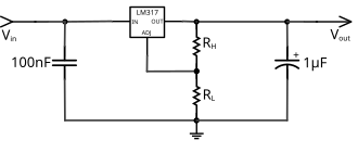
The LM317 has three pins: INput, OUTput, and ADJustment. Internally the device has a bandgap voltage reference which produces a stable reference voltage of Vref= 1.25 V followed by a feedback-stabilized amplifier with a relatively high output current capacity. How the adjustment pin is connected determines the output voltage as follows.
If the adjustment pin is connected to ground, the output pin delivers a regulated voltage of 1.25 V at currents up to the maximum. Higher regulated voltages are obtained by connecting the adjustment pin to a resistive voltage divider between the output and ground. Then
Vref is the difference in voltage between the OUT pin and the ADJ pin. Vref is typically 1.25 V during normal operation.
Because some quiescent current flows from the adjustment pin of the device, an error term is added:
To make the output more stable, the device is designed to keep the quiescent current at or below 100 μA, making it possible to ignore the error term in nearly all practical cases.
Current regulator

The device can be configured to regulate the current to a load, rather than the voltage, by replacing the low-side resistor of the divider with the load itself. The output current is that resulting from dropping the reference voltage across the resistor. Ideally, this is:
Accounting for quiescent current, this becomes:
LM317 can also be used to design various other circuits like 0 V to 30 V regulator circuit, adjustable regulator circuit with improved ripple rejection, precision current limiter circuit, tracking pre-regulator circuit, 1.25 V to 20 V regulator circuit with minimum program current, adjustable multiple on-card regulators with single control, battery charger circuit, 50 mA constant current battery charger circuit, slow turn-on 15 V regulator circuit, ac voltage regulator circuit, current-limited 6 V charger circuit, adjustable 4 V regulator circuit, high-current adjustable regulator circuit and many more.
Compared to 78xx/79xx
The LM317 is an adjustable analogue to the popular 78xx fixed regulators. Like the LM317, each of the 78xx regulators is designed to adjust the output voltage until it is some fixed voltage above the adjustment pin (which in this case is labelled "ground").
The mechanism used is similar enough that a voltage divider can be used in the same way as with the LM317 and the output follows the same formula, using the regulator's fixed voltage for Vref (e.g. 5 V for 7805). However, the 78xx device's quiescent current is substantially higher and less stable. Because of this, the error term in the formula cannot be ignored and the value of the low-side resistor becomes more critical. More stable adjustments can be made by providing a reference voltage that is less sensitive than a resistive divider to current fluctuations, such as a diode drop or a voltage buffer. The LM317 is designed to compensate for these fluctuations internally, making such measures unnecessary.
The LM337 relates in the same way to the fixed 79xx regulators.
Second sources from Eastern Bloc
The LM317 has an East European equivalent, the B3170V, which was manufactured in the German Democratic Republic (East Germany) by HFO (part of Kombinat Mikroelektronik Erfurt). Also, in USSR was manufactured and most popular ICs K142EN12A and KR142EN12A. These ICs are functional analogues of the LM317
See also
References
- ^ U.S. Patent 4176308.: "Voltage Regulator and Current Regulator", filed September 21, 1977.
- ^ "KA317/LM317 3-Terminal Positive Adjustable Regulator" (PDF). Archived from the original on 17 December 2013. Retrieved 2013-12-17.
{{cite web}}: CS1 maint: bot: original URL status unknown (link) - ^ "LM317 3-Terminal Adjustable Regulator" (PDF). Texas Instruments. October 2014. pp. 11–16. Archived from the original (PDF) on 31 March 2015. Retrieved 31 March 2015.
- "LM117/LM317A/LM317-N 3-Terminal Adjustable Regulator" (PDF). August 2013. Retrieved 2017-08-28.
- "LM340-N/LM78XX Series 3-Terminal Positive Regulators" (PDF). March 2013. Archived from the original (PDF) on 18 April 2016. Retrieved 2017-08-28.
External links
- Band-Gap
- The Design of Band-Gap Reference Circuits: Trials and Tribulations – Robert Pease, National Semiconductor (shows LM317 design in Figure 4: LM117)
- LM317 Bandgap Voltage Reference Example (ECE 327) – Brief explanation of the temperature-independent bandgap reference circuit within the LM317.
- Datasheets / Databooks
- Voltage Regulator Databook (Historical 1980), National Semiconductor
- LM317 (positive), LM350 (3 Amp), Texas Instruments (TI acquired National Semiconductor)
- LM317 (positive), LM350 (3 Amp), ON Semiconductor
- LM317 (positive), STMicroelectronics
- LM337 (negative), Texas Instruments


